Interesting Tech Projects
Posts tagged antenna

868MHz PCB Antenna
Dec 30th
I recently had a need to design an antenna on a PCB for LoRa, an 868MHz long range, low power communications protocol. For this project I decided to use an off-the-shelf LoRa module that already contained an RF matching network. The only requirement was a 50 Ohm antenna that would work at the desired frequency. Space on the board was limited.
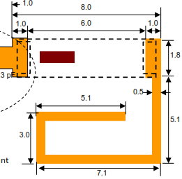
I decided to use a ceramic antenna to save space, selecting the Johanson 0868AT43A0020. The manufacturer has a datasheet showing how the part needs to be placed on a PCB.
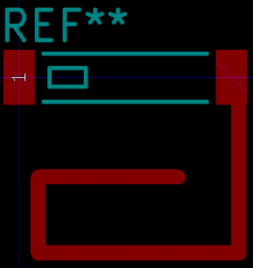
First step was to create a new PCB footprint containing the required layout.
The layout was followed precisely. I used the silkscreen to clearly indicate the orientation of the antenna. Note than only one end of the antenna is given a pin number. The other end is “no connection”. The schematic used a single pin connector component:
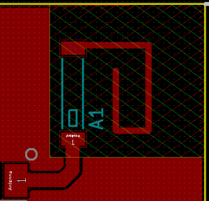
When laying out the PCB a “keep out” area was added to both sides of the PCB, making sure it extended 3mm beyond the antenna per the data sheet.
The track from the component pad to the antenna needs to have an impedance of 50 Ohms in order to minimize loss. It also needs to be surrounded by a ground area and have a ground area on the other side of the board. This is called a coplanar wave guide with ground plane.
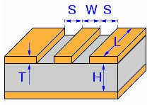
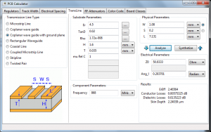
KiCAD has a built in calculator to work out the required track width in order to achieve 50 Ohms impedance. Here are the parameters I used for a standard 1.4mm FR4 two-layer PCB. I played around with the track width until I got close to 50 Ohms.
This gave a track width of 1.08mm when the gap between the ground and the track is 0.2mm (the KiCAD default).
- Er = 4.5 (FR4 PCB material)
- TanD = 0.02 (FR4 PCB material)
- Rho = 1.72e-008 (copper tracks)
- H = 1.6mm (standard two layer board thickness)
- T = 0.035mm (1oz copper thickness)
- S = 0.2mm (gap between ground pour and track on the track side of the board)
- L = 9.554mm (length of the track from pad to antenna)
- Frequency = 868MHz
